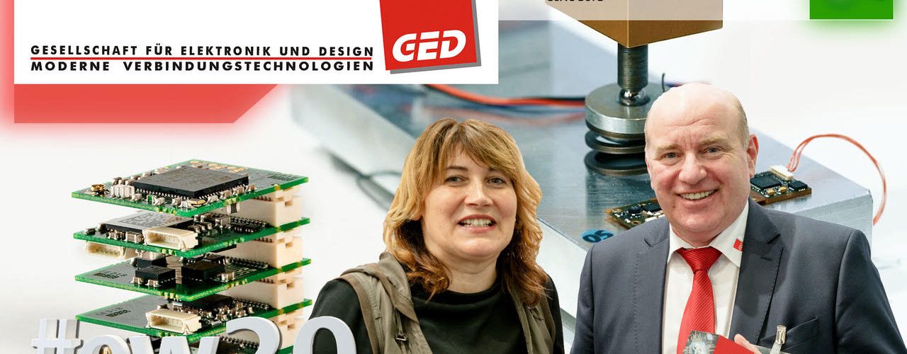
GED beherrscht Leiterplattenlayout, fertigungsgerechtes Design und gezielte Kostenoptimierung aus dem Effeff. Auf der Embedded World hat uns der Profi für Aufbau- und Verbindungstechnik den GED Sensor-Node vorgestellt. Der IoT-Sensor-Baukasten verknüpft Multisensorik, intelligente Datenverarbeitung und -Kommunikation mit flexibler Gestaltung auf minimalem Raum.
GED masters printed circuit board layout, production-oriented design and targeted cost optimization. At Embedded World, the professional for packaging technology introduced us to the GED sensor node. The IoT sensor kit combines multi-sensor technology, intelligent data processing and communication with flexible design in a minimal space.